There are various methods for preparing thin films. There are mainly physical vapor deposition (PVD) chemical vapor deposition (CVD), and sol-gel method and electroplating method in chemical solution coating are also more common.Next, we mainly talk about pvd coating and cvd coating.
PVD (Physical vapor deposition) is a film preparation technique. In a vacuum environment, through vacuum evaporation coating, sputtering coating, ion coating and other physical means, the coating material atoms or molecules are transferred from the source material to the substrate surface and deposited into a film. It has the advantages of high film purity, uniform and controllable thickness, strong adhesion, etc., and is widely used in optical, electronic, mechanical and other fields.
I.Magnetron sputtering coating
Principle: In a vacuum environment, the working gas (usually argon) is passed, and under the combined action of electric and magnetic fields, argon is ionized to produce argon ions. These argon ions bombard the target at high speed under the acceleration of electric field, so that the surface atoms of the target are sputtered out, and then deposited on the substrate surface to form a film. For example, when preparing ITO (indium tin oxide) films for touch screens, magnetron sputtering can precisely control the thickness and uniformity of the film.
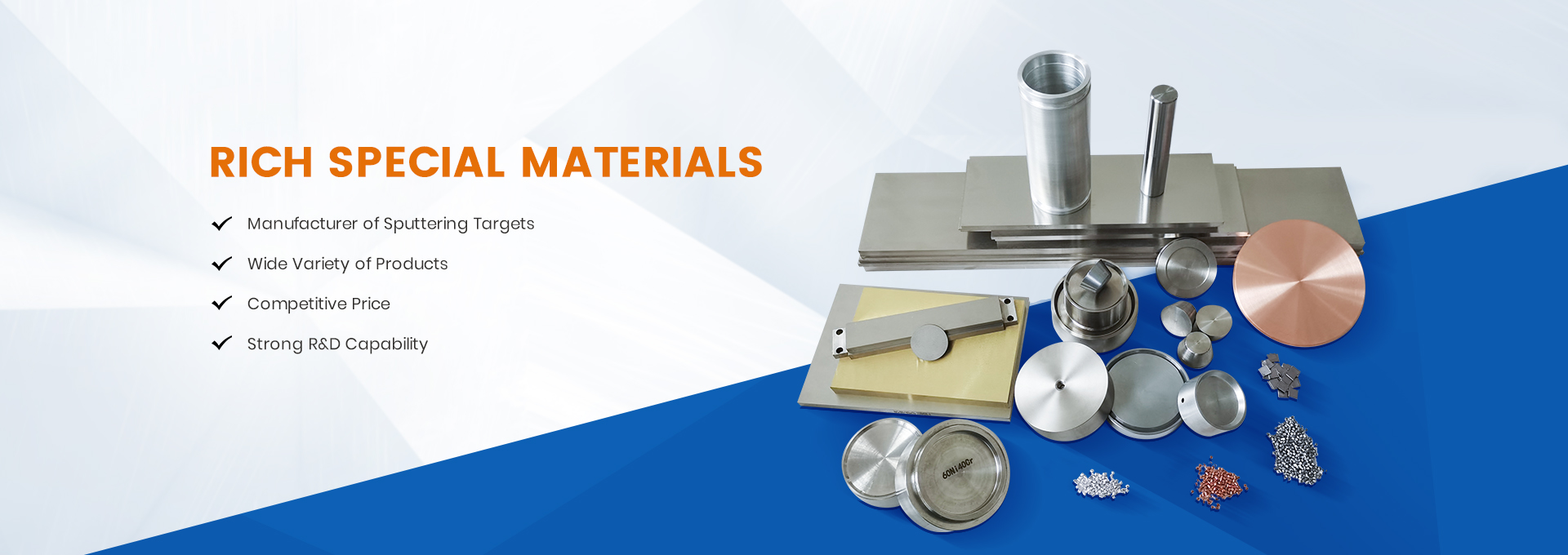
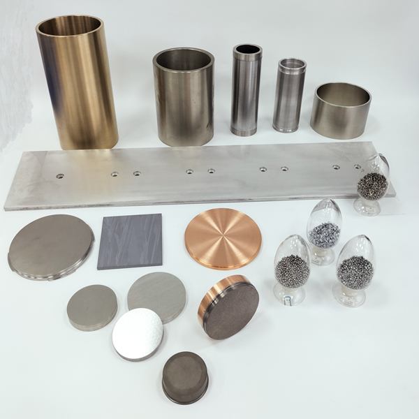
There are many kinds of targets commonly used for magnetron sputtering coating.
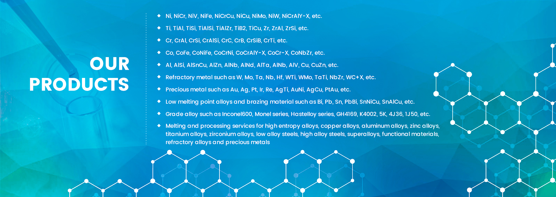
In terms of metal targets, there are aluminum targets, which are used in the electronics industry for integrated circuit metal wiring; Copper target material is an important material for metal wiring and printed circuit board manufacturing in advanced electronic devices. Titanium target material, widely used in aerospace and medical equipment fields, strong film adhesion; Gold targets for electronic electrodes, optical mirrors and jewelry decoration.
Alloy targets include nickel-chromium alloy targets for heating elements and sensors; Titanium-aluminum alloy targets are very important in the thermal barrier coating of aerospace engines.
II. Ion beam sputtering coating
Principle: The ion source is used to generate a high-energy ion beam to directly bombard the target, and the surface atoms of the target are sputtered out under the action of the ion beam, and then deposited on the substrate to form a film. For example, when preparing high-precision optical films, ion beam sputtering can make the films have high purity and precise thickness.
III.Electron beam evaporation coating
Principle: In a vacuum environment, the electron beam is used to heat the evaporation source (that is, the target), so that the target atoms or molecules obtain enough energy to change from solid to gas, and then deposit on the substrate surface to form a film. For example, in the preparation of metal mirror films, electron beam evaporation can quickly vaporize the metal target and form a film with high reflectivity on the substrate.
Chemical Vapor Deposition (CVD)
1.Atmospheric Chemical Vapor Deposition (APCVD)
Principle: Under atmospheric pressure, the gaseous reactants containing the film component elements are passed into the reaction chamber, and the gaseous reactants undergo chemical reactions on the surface of the substrate to generate a solid film and deposit on the substrate. For example, when preparing silicon carbide thin films, gaseous compounds containing silicon and carbon are used to generate silicon carbide thin films through chemical reactions.
2.Low pressure chemical Vapor Deposition (LPCVD)
Principle: In a low pressure environment, gaseous reactants chemically react on the surface of the substrate to form a thin film. Because the low-pressure environment reduces the probability of collisions of gas molecules, the reaction is more ordered, for example in semiconductor manufacturing for deposition of polysilicon films.
3.Plasma enhanced chemical Vapor Deposition (PECVD)
Principle: Plasma is introduced in the process of chemical vapor deposition, high-energy electrons and active groups in the plasma can activate gaseous reactants, reduce the temperature required for the reaction, and promote the deposition of thin films. For example, in the preparation of silicon nitride films, PECVD can achieve the deposition of high-quality films at lower temperatures, and is often used in the passivation layer of semiconductor devices.
Physical vapor deposition (PVD) and chemical vapor deposition (CVD) are two important coating technologies. PVD mainly includes evaporation, sputtering and ion plating methods, using a physical process to vaporize and deposit the source material on the substrate under vacuum conditions, with low deposition temperature, high film purity, strong adhesion and other advantages, often used in electronics, optics, decoration and other fields. CVD forms a thin film on the substrate through the biochemical reaction of the gaseous precursor at high temperature or under the action of plasma, and can achieve a large area uniform coating, which is widely used in semiconductor, aerospace and other industries.
Post time: Dec-30-2024

